
More than 400 layers: Micron skips a generation of flash memory
Micron is jumping straight from G9 to G11 in NAND memory, with the new chips set to store twice as much data per area. Volume production is planned for late 2027.
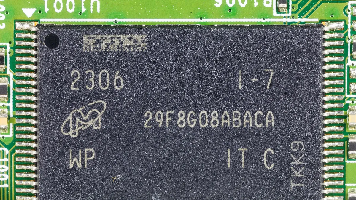
Symbolic image · Photo: Raimond Spekking / Wikimedia Commons, CC BY-SA 4.0 (cropped and resized)
U.S. memory maker Micron is skipping a planned generation of its flash memory. Instead of the intended generation with more than 300 layers, which was to be called G10, the company is moving directly from its current 276-layer G9 to G11 technology. Micron announced the move at a technology webinar for investors on Oct. 21, Blocks and Files reported.
G11 is to stack more than 400 memory layers and double bit density compared with G9. Data transfer is to be up to 50 percent faster, with more than 25 percent less energy per bit. To achieve this, Micron is relying on wafer-on-wafer bonding, according to Tom's Hardware: memory cells and control logic are made on separate silicon wafers using different processes and then joined. The company did not disclose the exact number of active layers.
“This G11 technology is the world’s most advanced NAND,” said Micron Chief Technology Officer Scott DeBoer. Volume production is to begin in the second half of 2027. Micron plans to give more details closer to the start of production. With new SSD designs, Micron is targeting AI applications in particular, according to Blocks and Files; the author, however, also sees the generational leap as marketing aimed at rivals such as Samsung and SK hynix.