
Crystals on demand: KAIST controls where ultrathin semiconductors start to grow
Korean researchers can pick the spot where a two-dimensional semiconductor crystal begins to grow, a step toward chips stacked in layers.
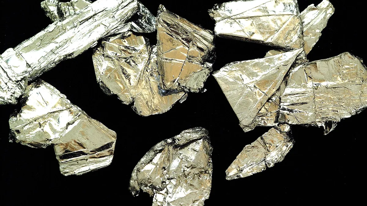
Symbolic image · Photo: Nessa Eull / Wikimedia Commons, CC0 (cropped and resized)
Researchers at South Korea's KAIST, working with UNIST, Hanyang University and TDS Innovation, have developed a method to decide exactly where a crystal of the atomically thin semiconductor molybdenum disulfide begins to grow. Such crystals normally form at random spots. “In thin-film growth, where a crystal forms is inherently a matter of probability,” said team leader Professor Kibum Kang. The findings were published Oct. 8 in the journal Nature.
The technique surrounds each patterned area with a hafnium oxide barrier. Oxygen released from the barrier suppresses the formation of new crystal seeds, most strongly near the edges and least in the center, so a single crystal starts growing at the chosen central point. This worked in more than 99% of 400 different patterns. The team also deposited a thin ruthenium film selectively onto regions of molybdenum diselenide.
The goal is chips in which computing and memory layers are stacked vertically, shortening the distance data must travel and potentially cutting delays and energy use. The semiconductor layers could be grown directly on existing circuits rather than grown separately and transferred. However, the researchers have not yet demonstrated a complete stacked processor, and it remains unclear whether the method can scale to mass production.