
Stacked transistors: IBM and Siemens team up to advance 3D Nanostack chip design
IBM and Siemens aim to ready IBM's stacked-transistor Nanostack architecture for volume manufacturing. Nearly 100 billion transistors already fit in a fingernail-sized area.
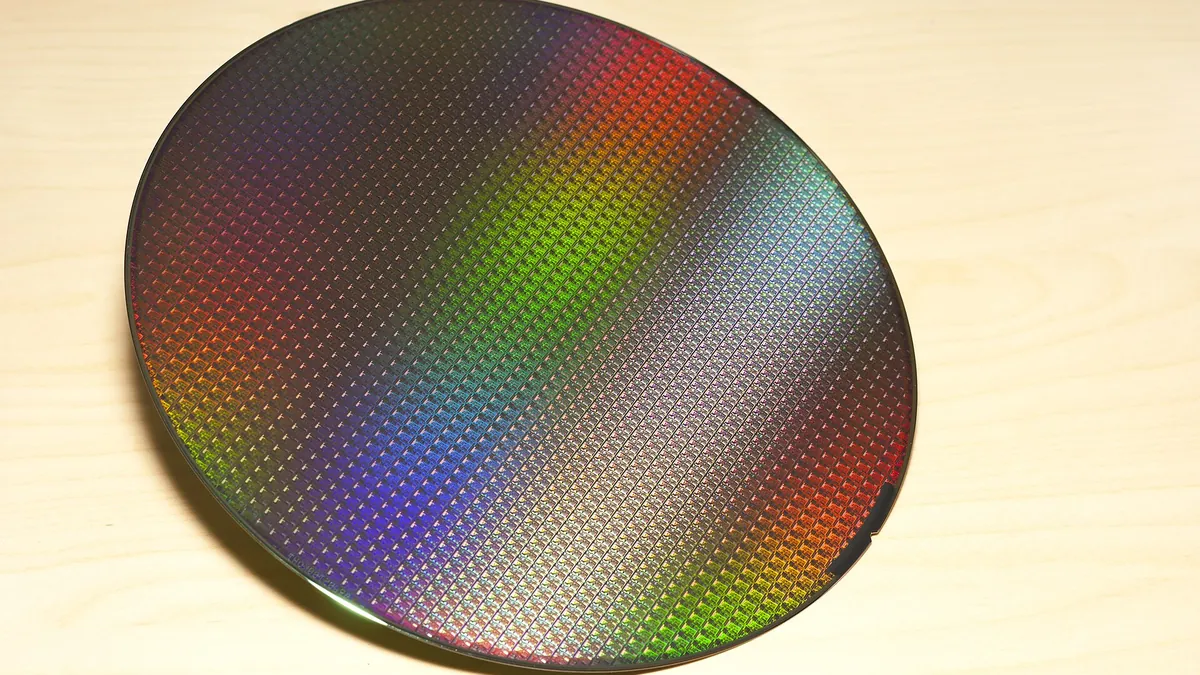
Symbolic image · Photo: Rob Bulmahn / Wikimedia Commons, CC BY 2.0 (cropped and resized)
IBM and Siemens on Wednesday announced a research collaboration on IBM's Nanostack chip architecture. The design, unveiled earlier this year, stacks and staggers nanosheet-based transistors vertically. At the current 7-angstrom node, it fits nearly 100 billion transistors into an area the size of a fingernail.
IBM contributes device research, while Siemens brings its electronic design automation (EDA), process simulation, lithography optimization and manufacturing software. The goal is to prepare the technology for large-scale production after proving it viable. Virtual models will test performance and fabrication challenges before chips are built, including for generations beyond 7 angstroms.
Huiming Bu, IBM's vice president of silicon technology R&D, said Nanostack represents the path forward for the logic scaling needed to support AI and other emerging technologies over the coming decade. The stacking is meant to deliver more AI computing power in a smaller footprint. Siemens executive Ankur Gupta called the design a pivotal leap forward.